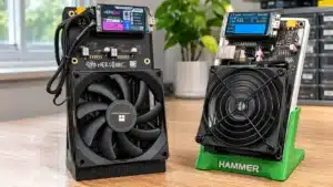
Ember One is an open-source Bitcoin mining hashboard reference design maintained by The 256 Foundation. EmberOne/00 places twelve Bitmain BM1362 ASICs on a 125 × 125 mm board. It needs a separate host controller, compatible mining software, a suitable power supply, and cooling to become a working mining system.
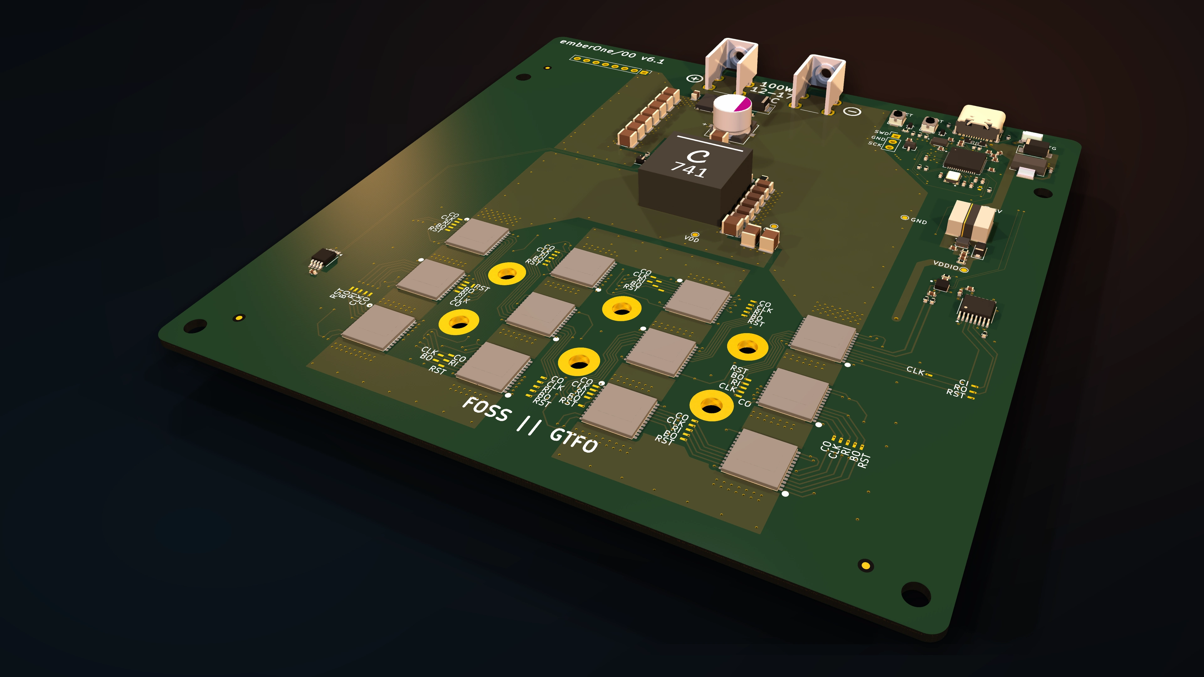
This guide follows the published v6.1 design files. That revision still needs board validation and measured performance testing; its 3.6 TH/s figure is theoretical. The board and circuit images are actual KiCad exports, not photographs or evidence of a completed build.
Reading the CAD markings: The source silkscreen still prints a 17 V upper input value. The project’s revision-specific guidance is 12–16 V DC for v6.1. A printed marking in a render does not override that limit.
Quick overview
- A hashboard, not a complete miner: Twelve BM1362 ASICs do the hashing; an external host runs the mining software and communicates over USB.
- Match the revision: This article illustrates v6.1. Its documented input is 12–16 V DC, while older revisions and outdated markings can show higher values.
- Separate targets from measurements: The project describes a 100 W power class and 3.6 TH/s theoretical nominal hashrate. It has not verified that hashrate on v6.1.
- Plan the complete system: Provide revision-matched power, cooling for the ASICs and power circuitry, a controller, and compatible software. The hashboard has no fan connector.
- Inspect the real design: KiCad files expose the six copper layers, power circuit, RP2040 USB interface, ASIC chain, and temperature-sensing circuits. Open files make the design inspectable; they do not establish measured performance.
What Is Ember One?
Ember One is The 256 Foundation’s published hardware reference design for a Bitcoin mining hashboard, intended for builders, researchers, and developers who want to inspect or develop the hashing hardware. The EmberOne/00 design uses twelve BM1362 ASICs and separates the hashboard from the host that manages mining.
A hashboard carries the application-specific integrated circuits, or ASICs, that perform mining work. A complete miner also needs a controller that receives jobs, communicates with those chips, and manages the system. Many assembled Bitaxe designs integrate an ESP32 controller on the mining board; Ember One instead exposes a USB interface to a separate host.
Published board files let readers examine the circuit and physical layout. That does not make the Bitmain ASIC itself an open chip design or establish an independent supply of ASIC silicon. The distinction matters in discussions of ASIC chip independence.
Ember One at a Glance
The figures below describe the v6.1 reference files and the project’s published status, rather than a benchmark or an individual manufactured board’s guaranteed performance.
| Specification | v6.1 reference design |
|---|---|
| Board type | Open-source Bitcoin mining hashboard |
| ASICs | 12 × Bitmain BM1362; BM1362AC footprints in the design |
| Power class | Approximately 100 W; actual operating draw depends on the build |
| DC input | 12–16 V DC in the project’s revision-specific guidance |
| Hashrate | 3.6 TH/s theoretical nominal; not yet verified on v6.1 |
| Board outline | 125 × 125 mm |
| PCB design | Six copper layers; nominal 1.6 mm thickness in the board file |
| Core regulator | U2: TPS546D24S in the actual schematic and PCB; see the source distinction below |
| Board interface | RP2040 running USB-serial firmware; USB connection to a separate host |
| Temperature sensing | TMP1075 and TMP451 circuits in the Data schematic |
| Cooling | Not included as a validated heatsink or water-block design; no fan connector on the hashboard |
| Hardware license | CERN-OHL-S-2.0 |
Power requirement: Check the exact board revision and the project specifications before connecting a supply. The 17 V marking visible in the v6.1 CAD files needs correction; older 12–24 V descriptions do not apply to this revision.
Inside the v6.1 Design
The board combines twelve ASIC positions with a core power stage, DC input terminals, an RP2040 USB interface, and temperature-sensing circuits. The five regions below help connect the physical layout to the schematic.
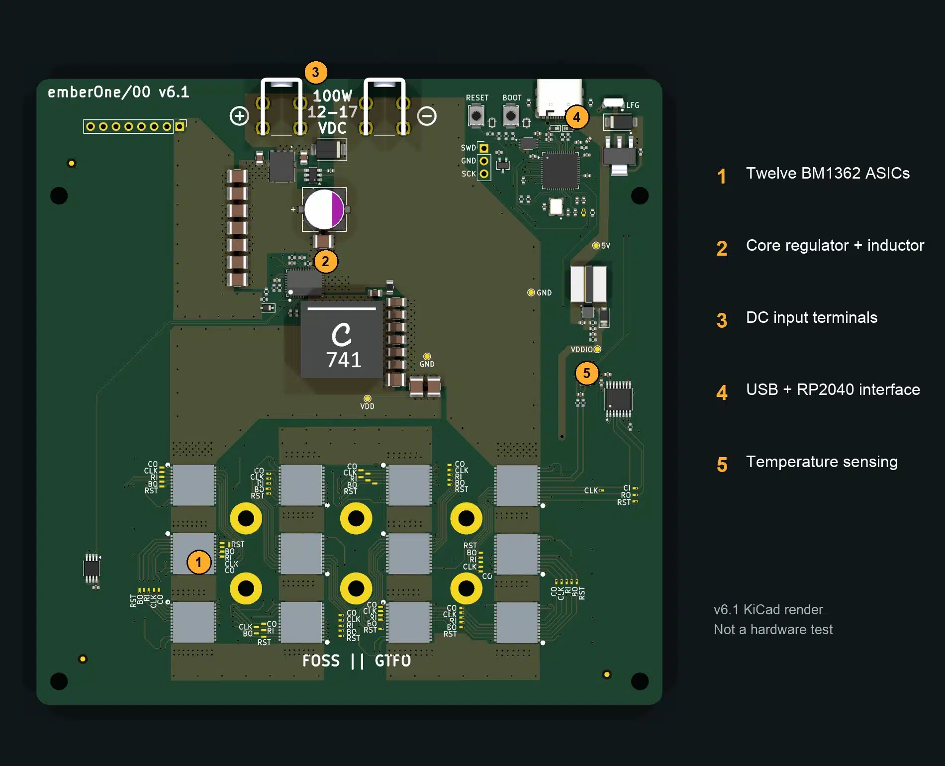
- 1. Hashing area: The twelve ASIC positions appear in four physical groups of three.
- 2. Core power: U2 and the large L1 inductor belong to the ASIC power supply.
- 3. DC input: J1 and J2 are the board’s positive and ground screw terminals. The USB connector is a separate interface.
- 4. USB and board interface: The upper-right region contains the USB connector, RP2040, and supporting circuitry.
- 5. Temperature sensing: U13 sits near the right edge, while U6 is near the lower-left edge. Read their exact connections in the Data schematic.
How the Twelve ASICs Connect
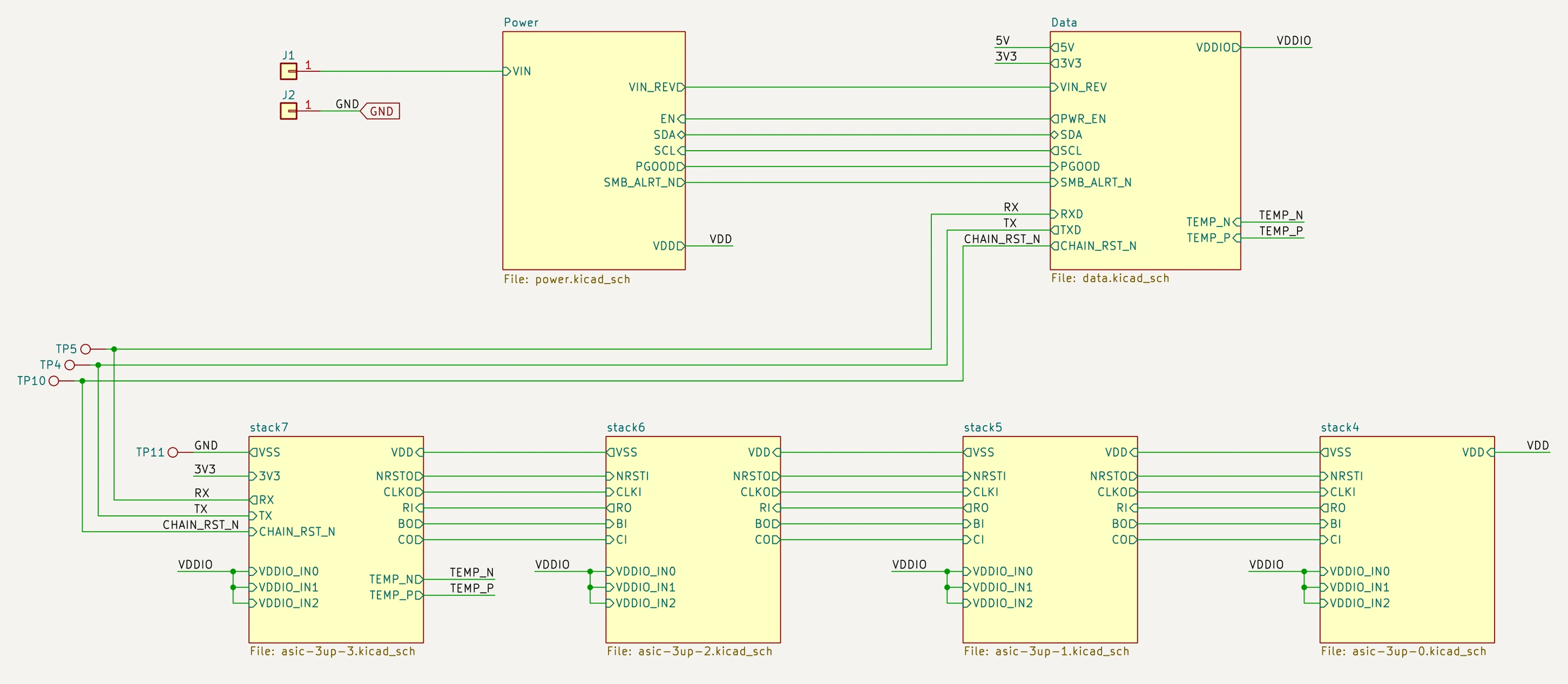
The published schematic organizes the twelve ASICs into four linked sheets, each containing three chips. The parent sheet connects the stack supplies and the clock, data, and reset signals; the drawing’s sheet boundaries do not represent four independent miners.
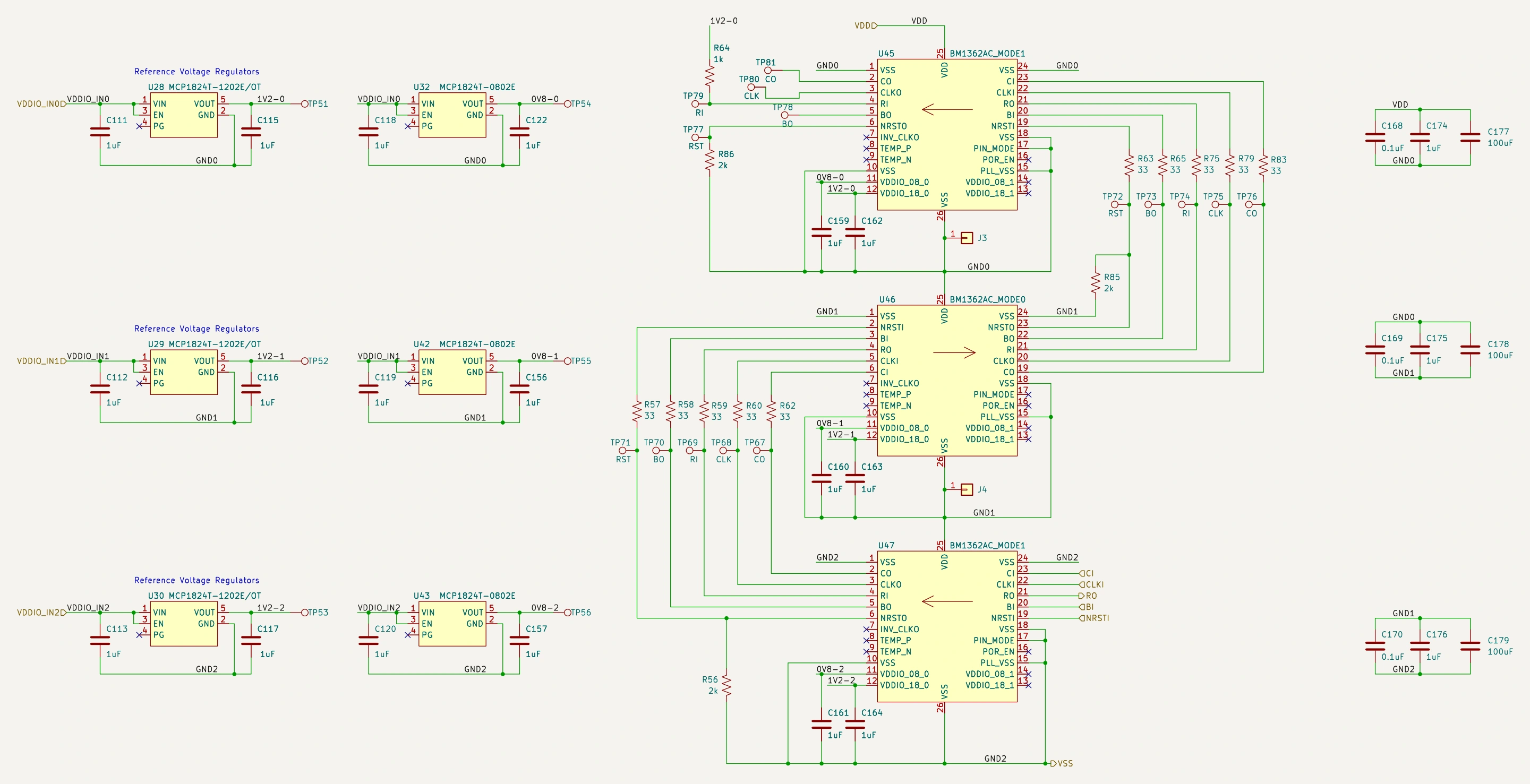
Inside a three-chip sheet, each ASIC has local supply references and supporting components. The source’s VDD, VSS, and intermediate ground labels must be read in context across the hierarchy. They are not instructions to connect the external DC input directly to an individual ASIC.
What the Six-Layer PCB Shows
The v6.1 board file contains six copper layers: F.Cu, In1.Cu, In2.Cu, In3.Cu, In4.Cu, and B.Cu. Looking at them separately reveals routing, copper regions, pads, and vias that a component-side render can hide.
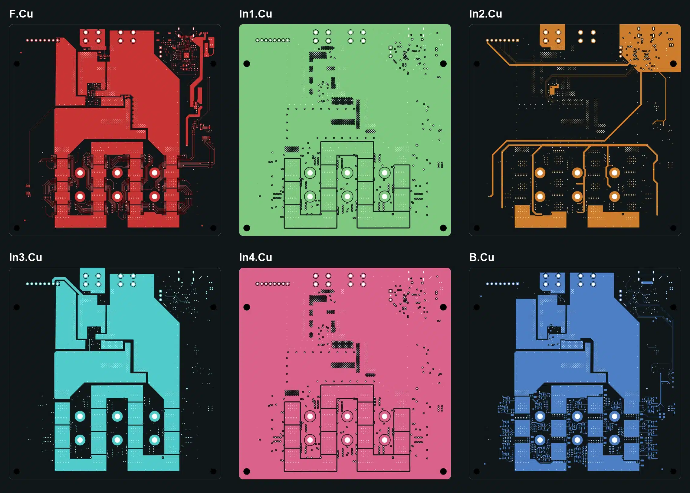
These plots come from the actual pinned v6.1 PCB layout. Every panel uses the same top-down project orientation, including B.Cu. Colors identify layers; they do not show temperature, measured current density, or electrical validation.
The nominal 1.6 mm thickness and copper stack are design-file properties. A fabrication order still needs the correct source revision and manufacturing requirements. A render or exported plot alone does not establish that an assembled board passes electrical or thermal tests.
How to Read the Power Schematic
The v6.1 Power sheet shows the input protection circuit, U2 core regulator, L1 inductor, and surrounding capacitors and control connections. It explains the circuit’s organization, not a complete wiring or first-power-on procedure.
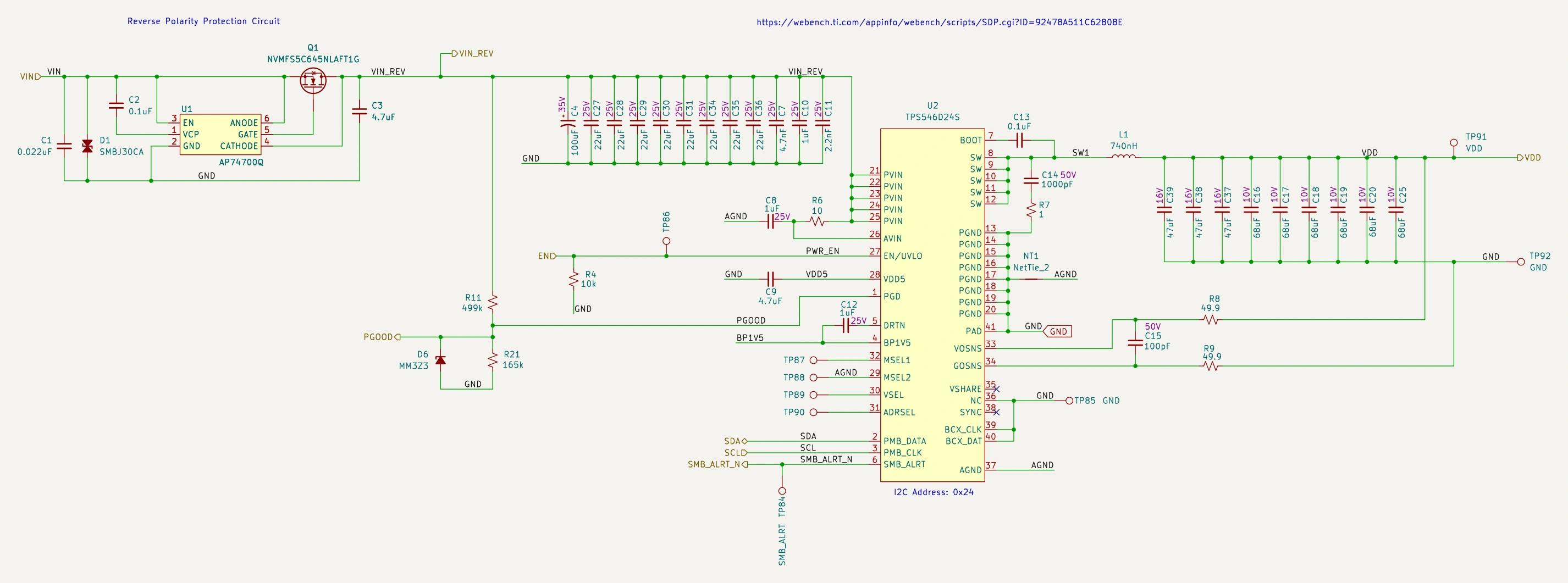
Regulator identity: Both the actual v6.1 power schematic and the PCB label U2 TPS546D24S. The project’s summary specifications name TPS546D24A. Those references differ, so identify the source-file part and the actual populated component rather than treating the summary as a bill of materials.
The Texas Instruments TPS546D24S specifications give a 16 V maximum for PVIN, the power-stage input. The separate AVIN controller supply can support 18 V; that does not raise the PVIN limit. The project’s 12–16 V DC guidance therefore remains the relevant input range for this revision.
The Internal 6 V Rail Is a Different Supply
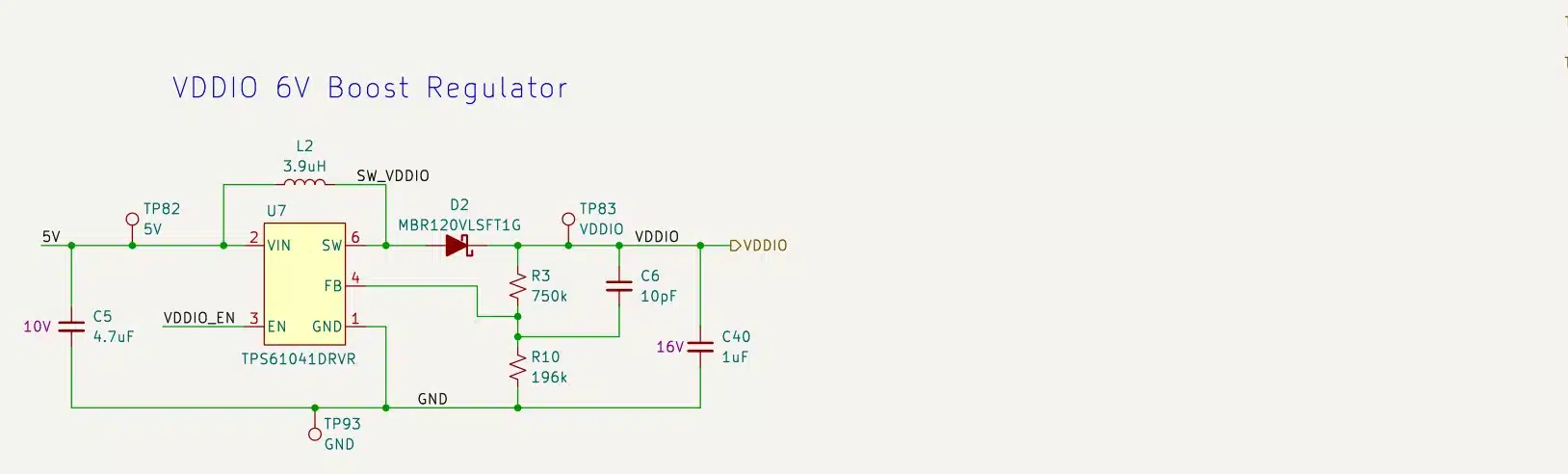
The Data sheet labels U7’s TPS61041 circuit as a 6 V VDDIO boost regulator. VDDIO serves the board’s internal interface circuitry; its 6 V label is not a replacement input-voltage recommendation for the whole hashboard.
Power: Check the Revision Before Connecting Anything
Use the documented 12–16 V DC range for v6.1, and confirm the actual hardware revision before selecting a supply. Earlier materials discussing 12–24 V or the v6.1 silkscreen’s 17 V upper marking must not override the revision-specific limit.
The source labels J1 as the positive input and J2 as ground. Connector polarity, conductor and connector ratings, and protection must match the build. Our Mean Well power-supply guide explains matching a supply’s voltage, connection, and load requirements; it is not approval to use an arbitrary model with Ember One.
The approximately 100 W figure is a power class, not measured wall consumption for every complete system. A host and cooling add loads, and the supply introduces conversion losses. Measure the actual system if you need wall power or operating cost. For household AC circuit planning, the home-mining electrical planning guide covers a separate question from this board’s DC input limits.
Cooling and What a Complete System Needs
The v6.1 reference design does not include a validated heatsink or water-block design, and the hashboard has no fan connector. Builders must provide cooling appropriate to the ASICs and power circuitry, then validate temperatures and stability on the actual assembly.
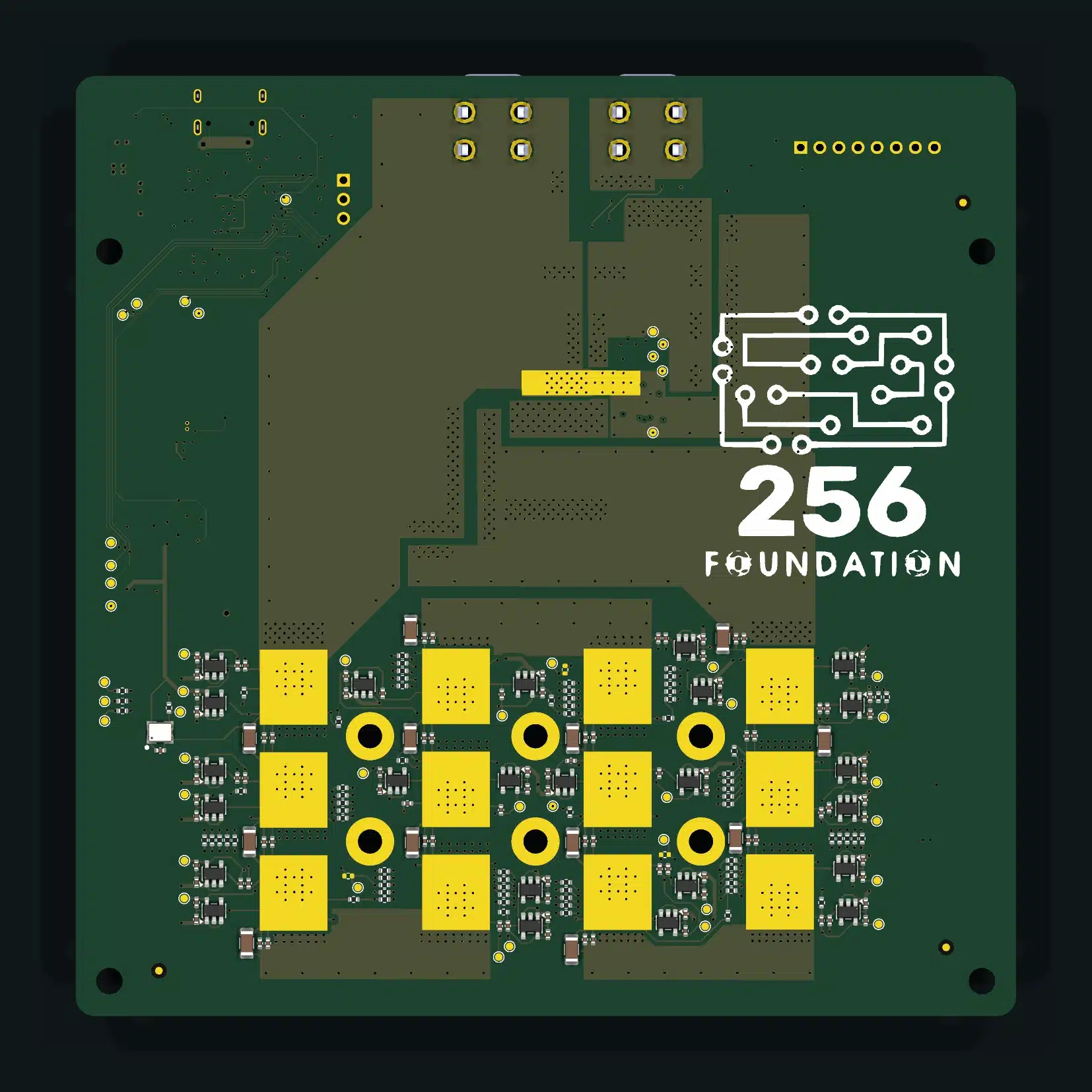
The underside view shows real layout features, including pads, vias, mounting holes, and board artwork. Their appearance does not establish heatsink contact, mounting pressure, electrical clearance, or cooling performance. A control board’s fan connectors also do not provide a thermal solution for the hashboard itself.
What Each Part of the System Does
A working system needs the hashboard, a compatible host, revision-matched power, suitable cooling, and mining software. The host connects to the mining service over the network and to the hashboard over USB.
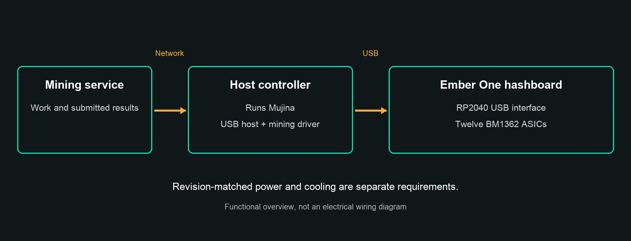
- Hashboard: EmberOne/00 carries the mining ASICs and board interface.
- Host controller: A separate compatible controller runs Mujina and the relevant board driver.
- Power: A regulated supply and wiring must suit the actual revision and complete load.
- Cooling: A suitable thermal assembly must serve the relevant components and operating conditions.
- Mining service: The selected pool or solo-mining backend supplies jobs and receives work. Its reward method and payout conditions remain separate from whether the hashboard is functioning.
What the Temperature Sensors Establish
The Data schematic includes U6 TMP1075 and U13 TMP451 temperature-sensing circuits. Those are monitoring components, not proof of acceptable temperatures or a validated cooling design.
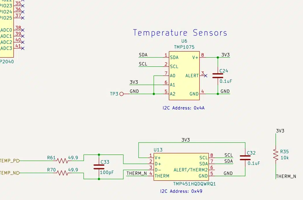
Read sensor values with the driver and hardware configuration in mind. A successful USB connection or detected sensor does not by itself demonstrate sustained hashing, correct cooling, or long-term reliability.
Firmware: Mujina and the USB Interface
Ember One uses two software layers with different jobs: USB-serial firmware on its RP2040, and Mujina on the separate host. The RP2040 interface does not replace the host’s mining software.
The Mujina compatibility matrix lists EmberOne/00 as working in mainline and notes that its driver is being reworked and remains under active development. That is software-support status, not a measured-performance or validation claim for every hardware revision.
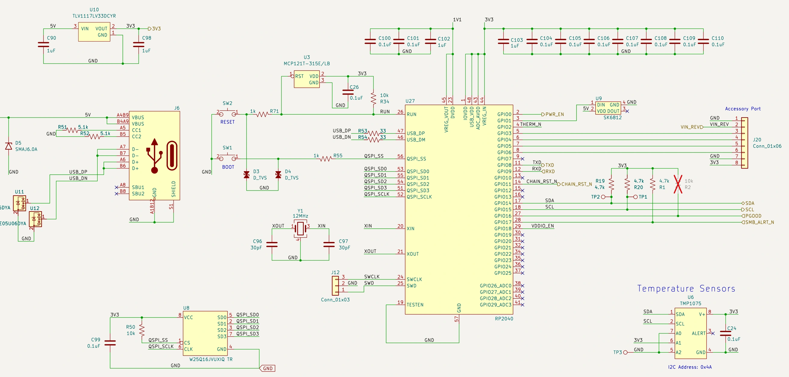
The Ember One USB-serial firmware runs on the board’s RP2040. The published USB interface reference describes two serial interfaces: one for control functions such as I2C, GPIO, ADC, and LED control, and another that passes UART data to the ASICs. The source-defined USB identity is VID:PID 1209:256f.
The firmware’s reported USB device revision is not a substitute for inspecting the hardware. The interface documentation explains that its bcdDevice constant encodes a hardware/firmware convention; do not infer that a v6.1 render proves the revision of a connected board.
The project does not publish a v6.1 bring-up or flashing procedure. Start from the project’s current Mujina guidance and compatibility information rather than applying a Bitaxe firmware file or unrelated web-flashing sequence. For the broader distinction between open code, compatible drivers, and the software actually running a miner, see why open-source mining firmware matters.
Is the 3.6 TH/s Figure a Measured Result?
No. The project lists 3.6 TH/s as theoretical nominal for v6.1 and says it has not been verified on that revision. Earlier boards have mined, but those demonstrations and historical test results do not establish a v6.1 benchmark.
The v3 release notes report 2 TH/s at a 500 MHz hash frequency and 3.4 V using test firmware. Those conditions belong to that historical v3 test; they are not v6.1 settings or a replacement for its documented external input requirement. Hashrate, power, thermals, and stability need measurement on the actual revision, controller, software, and cooling configuration.
Do not combine the nominal 100 W power class with an unverified hashrate to present a measured efficiency or a mining return. This article reports design-file findings and attributed project statements, not a Solo Satoshi performance test.
Revisions, Design Files, and Open-Source Licensing
The project identifies v6.1 as its latest design revision, while v3 remains the only formal GitHub Release. A newer development branch is not the same thing as a validated production release.
The project status page states that v6.1 still requires board validation and measured performance testing. It also identifies gaps in the build documentation and cooling design. Those limits matter even though earlier Ember One systems have operated.
| Revision or source | What it establishes | What it does not establish |
|---|---|---|
| v3 release, April 30, 2025 | A formal release with working-hardware claims and an attributed 2 TH/s test result | Performance, cooling, or input limits for v6.1 |
| v6.1 development branch | The latest reference-design files described by the project | Completed board validation or a verified 3.6 TH/s result |
| Mujina mainline support | A working EmberOne/00 software driver with active development | Identical behavior for every build or a finished consumer mining system |
Ember One Revision Timeline
The project’s revision history records the following milestones. Dates describe design work or releases, not a claim that every revision was fully validated.
- v1, October 2024: Early voltage-regulator test boards.
- v2, February 2025: The first full hashboard design.
- v3, April 30, 2025: The formal GitHub Release with historical working-hardware test notes.
- v4–v5, 2025: Protection, interface, and regulator changes across subsequent branches.
- v6–v6.1, 2026: Later development, including the 6 V VDDIO circuit and supervisory/control changes. The project still calls for v6.1 validation.
Which Files to Inspect
Use the v6.1 KiCad source branch for the design illustrated here. The default master branch is older, and its README contains outdated input-voltage and software-support statements.
emberone00.kicad_pro: The KiCad project.emberone00.kicad_pcb: The physical board layout, copper stack, pads, and routed geometry.emberone00.kicad_schand child sheets: The root schematic, Power and Data sheets, and ASIC-stack connections.3d/: Component models used by the reference render. A model is a visualization asset, not evidence of assembly or operation.
The project’s design-file guide says users generate manufacturing outputs in KiCad to suit their manufacturer. It also notes that the v6.1 README’s assembly-guide link points to a file absent from that branch. Do not treat an older assembly document as a validated v6.1 build guide.
The hardware is published under the CERN Open Hardware Licence Version 2, Strongly Reciprocal. The separate USB-serial firmware uses GPLv3. Credit for the hardware source belongs to Ember One contributors and The 256 Foundation.
Board and circuit visuals derive from commit 35e23434d6d79db4a1bdf17737916948826b748c using KiCad 10.0.1. They depict the published v6.1 reference design. The system diagram is a functional illustration. Neither is a photograph or a measured hardware result.
Who Is Ember One For?
Ember One is most useful to hardware developers, builders, and technically experienced miners who want to inspect or develop an open hashboard design. It requires more system integration and validation than selecting an assembled miner with a documented controller and cooling configuration.
Before planning a build or evaluating a board, establish the exact revision, validation evidence, required host software, power requirements, and cooling solution. The reference files alone do not establish the contents, condition, or support of any individual manufactured board.